BBC Micro RAM/ROM board
Back in the day, I got a Soldisk 2Mhz 128 board for my Beeb. It works
well; let's me have 8 ROMs in my machine, and 128K SWR RAM. It also lets
me use some of that RAM for "shadow" memory (similar to B+/Master). It's
quite a neat board.
Now I have a second Beeb, I wanted something similar. IFEL recently
released a RAM/ROM board. It's a variation on this theme; it uses up
all the ROM slots, but allows a 27512 to be used (4 ROM images). It
also has 64K of flash to store another 4 images. And 128K of RAM for
SWR. No shadow, but...
I've bought from this guy
before (2 TurboMMC boards and a Master Dual-OS system) and I like what
he does, so I gave it ago.
First thoughts
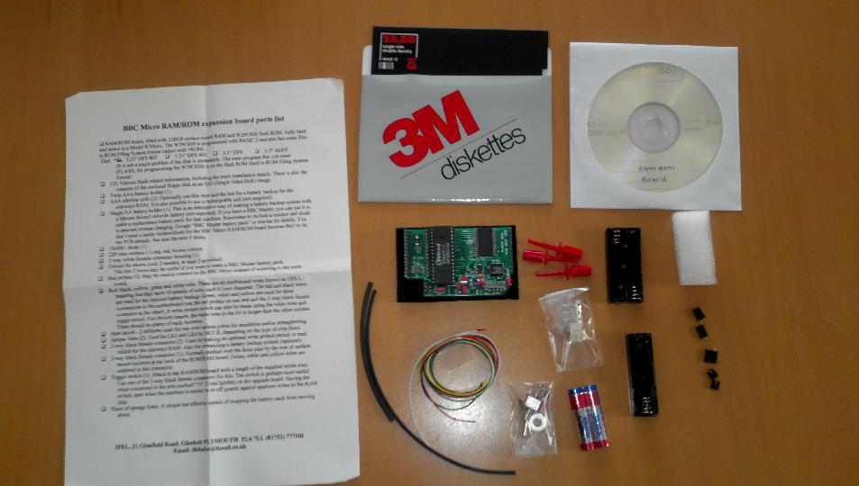
First glance; wow, it comes with lots of stuff!
The board itself; a floppy with software; a CD with install instructions
and software; twin AAA battery holder; 2 AAA batteries; single AAA battery
holder, diode, resistor, connector, crimps, probes, 5 wires, 2 sizes
of heat shrunk, jumpers, connectors, toggle switches and sponge foam!
Whoa, that's a lot of parts!
Hang on... those wires.. they're not stripped. Huh? Let's read the
install PDF. 53 pages! That can't be right... oh... 9 pages for install
(including lots of detailed pictures) and 44 pages of "how to use the
special features". That's an impressive document.
Now why are there so many components? Part of that is sheer flexibility.
Steve provides the parts so you can use different sized ROMS on the
board, battery backup of RAM, rechargeable lithium battery backup (also
usable on a Master to replace the original battery pack), write-protect
switch... very flexible.
But this flexibility comes at a cost; none of the components are
connected up. You need to solder the wires to connectors and to probes
(or directly to ICs). You have to solder more wires to connector and
write-protect switch. More to the battery pack. The heat-shrink is
to make these solder connections look good, and can also be used to hold
the cables together along their length.
Now I can understand why Steve did it this way; it's flexible and allows
the end-user to cut wires to exactly the size needed. Or to decide if you
want to run the cables above or below the motherboard (connect underneath
and it looks neater). If he had pre-soldered stuff then you might end
up with loose cables or a mess. And, you know, I would rather have
done that. I have the soldering skills of a demented monkey on crack.
I don't have the tools needed to use heat-shrink. I don't even have
a good wire stripper. Compared to other kit I've bought from Steve,
where the cables _were_ pre-soldered, this is a little disappointing.
Installation has gone from a 20 minute task to a major undertaking
(for me; I'm not even sure where my soldering iron is!).
Anyway, Steve appears to have put a lot of thought into this board
and the failure modes (eg what is the SWR gets corrupted and prevents
a boot?) There's a "inhibit" link that stops it from being read if
removed, so you can control-break, then replace the link, then erase/fix
the problem.
I don't want battery backup for my RAM, but I do want the ability to
write-protect all 8 banks; Steve's instructions allow me to (hopefully)
configure the board this way.
Obviously I can't help but to compare this to the old Solidisk 2Mhz that
I bought, back in the day. This sat in the 6502 socket, provided 128K
of RAM and 4 extra ROM slots. The RAM could be configured as SWR or
as shadow. Steve's board _removes_ ROM slots, but you can put a 27512 in
socket B to have 4 images; you can use the flash to store 4 more images or
replace it with another EPROM (eg another 27512). Except for 'shadow',
Steve's board seems almost as flexible as the old Solidisk board. And,
really, I never used shadow much! It wasn't totally B+ compatible and
required a lot of kludges. One win for the Solidisk board though; this
also has wires that need plugging in, but they came with the necessary
connectors; no soldering necessary.
Now to set fire to things and connect up wires, and see how the board
works in practice!
Partial installation
Initially I soldered together the 3 cables needed to connect to the
necessary ICs. I only burned myself once. The result is my normal
expected fragile-looking (look at it and it'll break) mess. These cables
are very thin. Annoyingly on my model-7 board these ICs are not socketed.
Using the probes is a pain... but I think I managed to get them connected
without shorting out anything.
I note that two of the probes have to sit under the keyboard and they
stick up too high. Hopefully when I tighten the keyboard down then
they'll stay put.
Inserting the main board was a real pain. Because of the mounting screws
on the motherboard, pushing down on the far-right of this RAM-ROM board
caused a scary amount of flex. I was half afraid I'd break something!
It took me three attempts to get the board seated... and then I wasn't
quite sure it was in place properly.
I'll not be surprised if this machine develops intermittent faults.
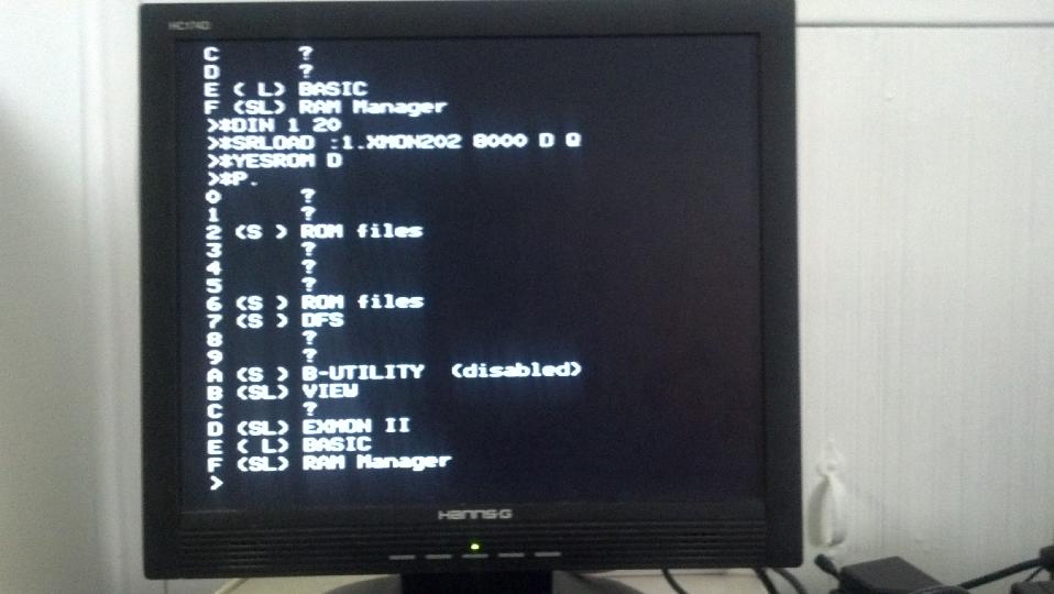
Test 1: Insert a 27128 with the TurboMMC ROM on it into the spare socket.
Power up. Huh, OK, so it says 32K and TurboMMC wakes up and I can see my
MMC card. OK. I don't have a BASIC ROM in this machine now, so it must
be loading that from FLASH. *HELP shows a B-Utilities ROM. *ROM and
I see two RFS ROMS. CHAIN "TEST1" and it says it finds 8 ram banks;
FLASHER fails because BASIC is running from FLASH. So far, so good!
I replaced the 27128 with a 27512 (BASIC, MMC, VIEW, my Manager ROM)
and power up. 224K RAM? And a crash. Huh. Some messing around later
and it seems as if my manager ROM is detecting the FLASH sockets as RAM.
Now the code that does that basically uses &FFB9 (OSRDRM - Read a byte
from paged ROM) to get the contents of &BFFF, they EOR's that with 255
then attempts to write it back (standard &F4/&FE30 process). It then
reads the value again using &FFB9; if it's unchanged then it's not RAM,
else it is. We then write back the original value. This, in theory, is
a non-destructive test; an interrupt at the moment might cause issues, but
that's why I selected &BFFF as my test address; least likely to be used!
However the manual does warn about attempts to write to the flash;
this should(!) fail but it can lead to the FLASH internal state machine
getting confused, and reads not returning the correct value. I'm guessing
that this is what is happening (perhaps the read is returning the value
attempted to be written) and that's why my ROM is killing the machine.
Except further tests don't seem to back this up; I physically removed the
WINBOND chip and got similar results. With no FLASH chip then on power-up
the machine still hangs, but on control-break then it detects the right
number of RAM banks and works properly. It also breaks after ?&FE4E=127
followed by BREAK. Hmm, OK, there was one difference; without the FLASH
chip then control-break returned the machine to normal operation; with
the FLASH insider then it didn't.
Despite this set back, the machine appears to be running correctly with
the lid off.
Bank mapping is a little weird; a consequence of how Steve is doing
address decoding.
0: RAM
1: RAM
2: Flash (defaults RFS "ROMfiles1" - utility programs
3: 27512 bank 0

4: RAM
5: RAM
6: Flash (defaults RFS "ROMfiles2" - test programs
7: 27512 bank 1

8: RAM
9: RAM
A: Flash (defaults to B-Utilities ROM)
B: 27512 bank 2

C: RAM
D: RAM
E: Flash (defaults to BASIC 2)
F: 27512 bank 3
Conclusion so far: Installation was a pig; worse than I expected, and
worse than anything I ever installed BITD (even the original Solidisk
SWR wasn't that bad and that hooked into the user port for RAM select).
The compatibility issue is a little worrying; I can rewrite my ROM so
it only probes known bank numbers (so it skips writing to FLASH), but
the possibility of FLASH writing breaking stuff is a little worrying.
I definitely need to look further into the boot-up sequence code in
my ROM to see if I can find out why it's breaking. (Maybe attempts to
write to FE34? The STL SWR 2M128 emulated ACCCON for shadow memory so
my ROM uses it as well. Hmm...)
And, indeed, this seems to be the main problem. I quickly NOP'd out
all writes to &FE34 and now the machine acts differently. It doesn't
crash... kinda
Still mis-detecting the number of SWR slots, but the machine is starting
up correctly.
Now Steve pinged me (two reasons I like buying from him; he makes
good stuff _and_ has excellent customer service) with an idea that a
200us delay after each write should be enough to let the flash recover. He
also suggested some other tests.
Part of the flexibility of this board is to write protect half the RAM
banks (link near R1), or all the banks (TWP). A side consequence of
the half-protection is that it should also write protect the flash. I
knew this wouldn't solve my problem 'cos it also broke with the Winbond
chip removed, but it then made a good test later; with it removed the
ROM correctly reports 96K RAM (64K SWR+32K main memory). And another
confusion resolved it; the B-Utilities ROM conflicts with my ROM in
terms of workspace (I use some locations marked as unused in the advanced
userguide; it seems B-Utilities uses the same space).
Next step is to see if a 200us delay resolves the Flash test
issue. It definitely seems as if the machine has recovered by the time
the OS is performing the rest of its startup process.
Hmm... what's the best way to do a 200us delay? A "DEY" uses 2 cycles;
a BNE uses 3 cycles, so "LDY #40 / .loop / DEY / BNE loop" would be
around 200us for a 2Mhz CPU?
Turns out a value of #&50 is too low; #&80 seems to work, for safety I
just did #00 (so effectively 256 loops). This does slightly slow down the
startup (the beep seems to be stretched... maybe, perhaps, or I might be
hallucinating!) but it consistently reports the correct number of banks.
My ROM is now binary patch (*TV) on top of binary patch (ACCCON) on top
of binary patch (delay after write for RAM detection). Yuck. I think I'm
gonna have to go back to the source and do this properly with conditional
compiles for STL (so SHADOW, SHPLUS, ACCCON routines). Maybe :-)
Finish up
Some more demented monkey soldering later and the write-protect switch is installed and working.
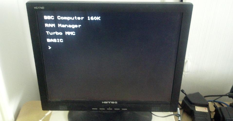
The basic commands in the ROM also work:
How it looks inside
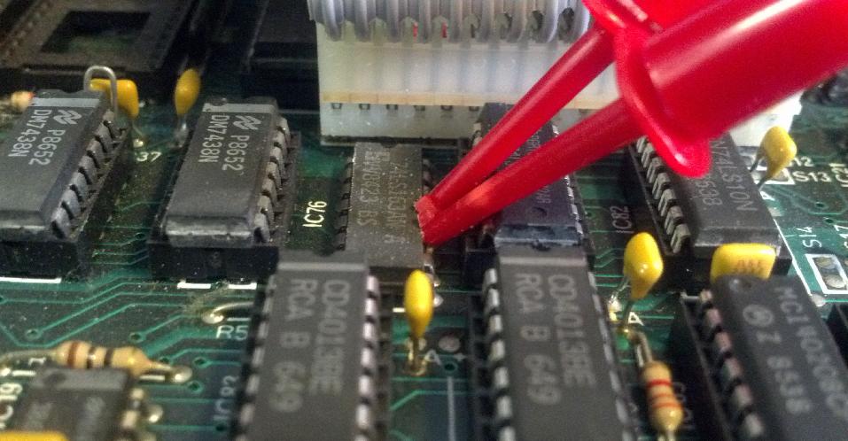
Probe on IC77
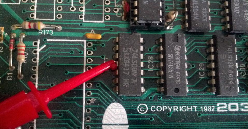
Probe on IC76
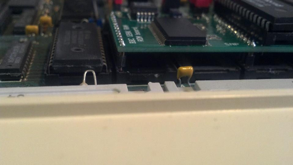
Main board - note that it's not 100% down in the sockets and part of the pins are still showing. It seems to be working, though...
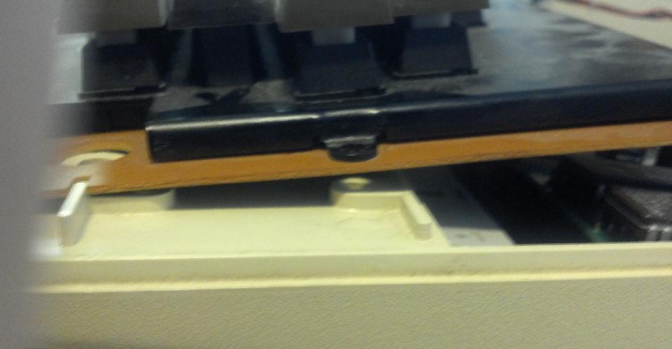
The probes on IC76 force the keyboard up; you can see a gap caused. Careful bending of the probes does allow the keyboard to screw down properly though
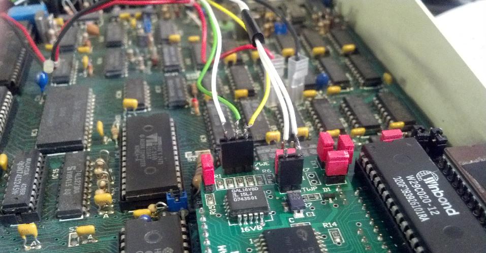
And the weakest part of the system - my demented monkey on crack soldering
Conclusion
This board is to Steve's high standards. Installation is a real pig;
pre-soldered cables and a better way of connection to the right ICs would
take this from "very good" to "excellent". The FLASH write issue is a
minor concern; given that the Winbond chip does recover after a short
period of time, I'm not sure this is a big risk; ROMs like mine misdetected
Flash as RAM, but didn't stop the system from running BASIC from Flash.
(The issues with ACCCON were all of my making).
Score: 11 SWR banks out of 16 (would score 13 if cables were pre-made; 15
if the main board was easier to insert). If you're not afraid of a
soldering iron then this board is just fine for your needs and I
recommend it. If you can make one work then you'll have a harder time,
but if I can get it working then almost anyone can!
ADDENDUM:
It seems the latest boards from Steve now have the cables pre-made (at
least the pictures in his ebay store shw the cables pre-made), which is
a big plus in my book. Good stuff!
Last modified: Sunday, 08-Sep-2019 13:41:19 EDT